
Marcy Nanocenter: Frequently Asked Questions
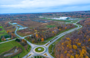
This FAQ addresses common questions about Marcy Nanocenter, including its campus profile, infrastructure, utilities, environmental review, and readiness for additional advanced-manufacturing development.
Key facts at a glance
- 434 acres of advanced-manufacturing campus space
- 127 acres currently available
- $1.2 billion public-private investment for the Wolfspeed Fab
- $165 million invested toward infrastructure and site improvements
- 112,000 square feet of cleanroom space in use with an additional 1 million square feet of cleanroom capacity
- 200 MW of current electrical capacity with expansion plans for an additional 200MW
- Two 24″ water mains, supplied by the Mohawk Valley Water Authority’s Hinkley Reservoir
- 3 miles to the nearest I-90 NYS Thruway on-ramp
1. What is Marcy Nanocenter?
Answer: Marcy Nanocenter is a 434-acre greenfield advanced-manufacturing campus in Marcy, Oneida County, New York, developed specifically to accommodate semiconductor and other high-technology manufacturing. It is currently home to Wolfspeed’s Mohawk Valley semiconductor fabrication facility, representing a $1.2 billion public-private investment, while the overall site and infrastructure investment in the campus is approximately $165 million. Marcy Nanocenter has undergone decades of planning, infrastructure investment, utility development, environmental review, and site preparation. Existing electric, water, transportation, wastewater, telecommunications, and natural-gas infrastructure reduce the amount of time required to prepare the site for future advanced-manufacturing projects.
2. Where is Marcy Nanocenter located?
Answer: The Marcy Nanocenter campus is located on the SUNY Marcy Parkway in Marcy New York.
3. What is already operating on the campus?
Answer: Wolfspeed’s 480,000 square foot, Mohawk Valley semiconductor fabrication facility is located at Marcy Nanocenter. In addition to this facility Marcy Nanocenter supplies a fully operational 200MW electrical substation and a newly constructed, 60,000 square foot flexible manufacturing/warehouse/office space, currently occupied by Danfoss and Indium Corporation.
4. How much additional development capacity is available?
Answer: Approximately 127 acres remain available, supporting roughly 2.7 million square feet of additional building footprint depending on final site design and infrastructure requirements. Of that 2.7 million square feet, 1 million square feet is reserved for cleanroom space and the rest accounts for office, warehousing, utility and other building areas. Marcy Nanocenter has adjacent supply chain property with approval to construct 90,000 SF of office, manufacturing or warehouse space.
5. Was the site designed specifically for semiconductor manufacturing?
Answer: Yes. Marcy Nanocenter is not a conventional industrial park being converted to accommodate semiconductor manufacturing. It has been planned, engineered, permitted and developed specifically for semiconductor and advanced-technology investment, including infrastructure, environmental planning, and cleanroom development capacity.
6. How much electrical power is available?
Answer: Marcy Nanocenter currently has 200 MW of electrical capacity, with a planned substation expansion expected to increase total capacity to approximately 400 MW. This number follows a previously planned substation upgrade project. Major new manufacturing projects would proceed through the appropriate utility and electric-grid planning processes. Electrical demand is projected to increase over time as facilities are constructed, equipped, and brought into production rather than appearing all at once.
7. Does a new project immediately use its full electrical demand?
Answer: No. Demand would increase gradually as construction is completed, equipment is installed, and manufacturing ramps up. Project-specific utility and electric-grid planning would be required.
8. Is there water infrastructure to support semiconductor manufacturing?
Answer: Reliable water infrastructure is incorporated into the planning of Marcy Nanocenter, consisting of two 24″ water mains. Mohawk Valley Water Authority can currently draw up to 32 million gallons per day. The authorized future withdrawal limit is up to 48.5 million gallons per day. Any future project’s water needs would be evaluated through engineering studies and utility reviews. Infrastructure planning occurs well before full production begins, and any necessary improvements would be identified through permitting and review processes.
9. Would a major new manufacturer immediately place its ultimate water demand on the regional system?
Answer: No. The addition of a major manufacturer would involve detailed planning and review. Existing and future system requirements, project-specific demand, capacity, and infrastructure improvements would be considered as part of infrastructure planning.
10. Are semiconductor facilities subject to environmental regulation?
Answer: Yes. Semiconductor manufacturing is subject to extensive environmental regulation. Marcy Nanocenter works closely with the New York State Department of Environmental Conservation (DEC), the U.S. Army Corps of Engineers (USACE), and other organizations, as needed, to ensure that all projects and site work comply with applicable environmental standards. The Town of Marcy, as lead agency for the campus, has previously approved the required zoning for Marcy Nanocenter. Environmental permits establish enforceable limits and monitoring requirements that facilities must comply with throughout operations.
Previous air permitting work at Marcy Nanocenter included air-dispersion modeling, emission caps, modeling of nitrogen dioxide and sulfur dioxide, evaluation of inorganic fluoride emissions, and demonstration of compliance with applicable air-quality standards. Beyond air permitting, site permitting and review requirements include stormwater runoff permitting under the State Pollutant Discharge Elimination System (SPDES), sedimentation and erosion control, zoning limitations such as setbacks and building heights, wetlands permits, and other permits specific to end users. Review under the State Environmental Quality Review Act (SEQRA) is also required.
11. Would a new semiconductor manufacturer require additional environmental review?
Answer: Yes. A new semiconductor manufacturer would require project-specific environmental evaluation and applicable approvals from the New York State Department of Environmental Conservation and other agencies with jurisdiction. Projects are reviewed in coordination with applicable federal, state, and local regulatory agencies to ensure compliance with environmental requirements and permitting standards. These agencies ensure a project meets the standards set in place to identify, measure, and minimize potential negative impacts on nature, public health, and local communities before construction starts.
12. Does the campus or a future facility produce “zero emissions”?
Answer: A semiconductor facility should not be characterized as producing “zero emissions.” Applicable emissions must be identified, evaluated, controlled, and maintained within legally enforceable permit requirements.
13. What infrastructure serves the campus?
Answer: The campus has electrical, water, transportation, wastewater, telecommunications, and natural gas infrastructure planned to support major advanced-manufacturing users, with current excess capacities. Specific improvements and capacity requirements for a new project would be evaluated through engineering, utility coordination, and regulatory review.
14. What is the overall significance of Marcy Nanocenter?
Answer: Marcy Nanocenter represents a sustained regional and state asset for establishing a semiconductor-ready manufacturing campus in Upstate New York. Strategically positioned within the growing Upstate New York semiconductor corridor, the campus reflects 30 years of planning, infrastructure development, and financial commitment, complementing investments across Upstate New York with the goal of strengthening domestic semiconductor supply chains. These investments demonstrate a long-term commitment to building an asset of regional, statewide, and national significance. Any future semiconductor project would build on this foundation while remaining subject to detailed engineering, utility coordination, environmental permitting, and regulatory oversight before reaching full production. The campus’s readiness for additional development is therefore supported by both its existing investments and the project-specific planning required to accommodate future manufacturing operations. Marcy Nanocenter is positioned for continued growth, with an ongoing commitment to adapting to the evolving needs of the semiconductor industry.
Closing note
Infrastructure demand and environmental requirements are project-specific and depend on the actual facility design, processes, equipment, construction schedule, and production ramp.
